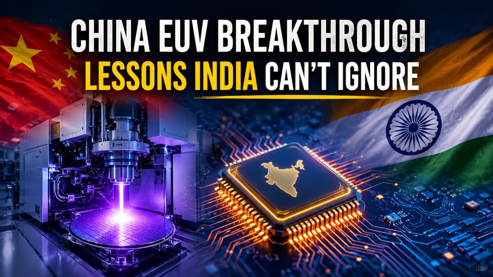
China’s reported progress in extreme ultraviolet lithography has intensified the global race for advanced AI chips. Although its prototype cannot yet manufacture usable semiconductors, the project highlights why India must invest in chip equipment, research and skilled manufacturing.
China EUV prototype reaches an important stage
China has reportedly assembled an indigenous extreme ultraviolet lithography prototype at a secure research facility in Shenzhen. The project involves state-supported institutes, technology companies and engineers with experience in advanced lithography systems.
The development is significant, but it should not be described as a completed commercial breakthrough. Reports indicate that the prototype can generate extreme ultraviolet light but has not yet produced functional chips. Researchers are reportedly aiming to demonstrate chip production by 2028, although 2030 is considered a more realistic target.
This distinction matters. Generating EUV light is only one part of an extraordinarily difficult manufacturing process. A production-ready machine must also combine advanced mirrors, wafer positioning systems, vacuum chambers, software and precise controls while maintaining acceptable yields.
EUV tech powers advanced AI chips
EUV lithography uses light with a wavelength of 13.5 nanometres to transfer extremely small circuit patterns onto silicon wafers. The shorter wavelength allows manufacturers to produce denser and more powerful processors used in artificial intelligence systems, smartphones, data centres and defence technology.
Dutch company ASML remains the only commercial supplier of complete EUV lithography systems. Its latest machines use highly sophisticated light sources and optical components that took decades of research, testing and industrial cooperation to develop.
China has been unable to purchase ASML’s EUV systems because of export restrictions. ASML confirmed in June 2026 that it had never shipped an EUV machine or components specifically designed for such a machine to China. These restrictions have pushed Beijing to accelerate domestic research into lithography, semiconductor materials and manufacturing equipment.
Export curbs reshape the chipmaking race
A commercially viable Chinese EUV tool could reduce the country’s dependence on foreign semiconductor equipment. It could strengthen domestic production for artificial intelligence, electric vehicles, telecommunications and military systems.
However, a laboratory prototype is far removed from high-volume manufacturing. China still needs to solve major problems involving precision optics, system integration, reliability and production yield. Chinese semiconductor executives have themselves called for stronger national coordination to connect progress in light sources, wafer stages, materials and electronic design tools.
Success could eventually challenge ASML’s position and weaken the long-term effectiveness of technology export restrictions. Failure to achieve commercial yields, however, would leave China dependent on older lithography methods for several more years.
India chips strategy needs deeper investment
India has expanded its semiconductor programme but remains focused mainly on fabrication, assembly, testing, packaging and chip design. As of May 2026, the government said 12 fabrication or packaging projects and 24 semiconductor design projects had been approved under the Semicon India Programme.
India Semiconductor Mission 2.0 aims to strengthen equipment, materials, research, design and advanced packaging. Earlier government data showed that approved projects represented investment of about ₹1.60 lakh crore by December 2025.
India’s weakness is not engineering talent but the absence of a complete advanced manufacturing ecosystem. Building a domestic EUV machine immediately may be unrealistic. A more practical mission would begin with materials, precision components, optics, metrology, packaging equipment and mature-node fabrication.
India needs patient funding, stable policies and long-term cooperation among universities, laboratories and private manufacturers. Subsidising factories alone will not create semiconductor independence. Genuine self-reliance will require domestic intellectual property, specialised equipment, experienced technicians and research programmes capable of surviving beyond one budget cycle.